Arm Cortex-M4 (2): ADC
- ➡️ #EmbeddedSystems #ARM #CortexM4 #CProgrammingLanguage #ADC #ADC_read #Nucleo #F446RE #STM32F446RE #MCU #STM32cube
- ⭐ Codes of practice:
- ⭐ Repository with more examples:
- ✅ Developed by:
- ➡️ Device:
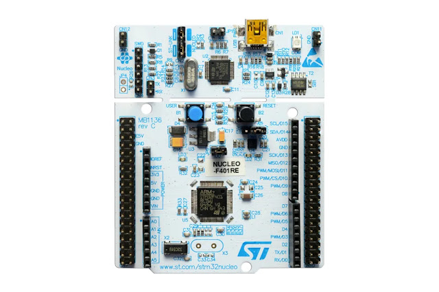
- Development Board: NUCLEO-F446RE
- Processor: STM32F446RE MCU, Arm® Cortex®-M4 core at 180 Mhz.
- ➡️ Compiler:
- ⭐ Device provided by:
- ⭐ When using this resource, please cite the original publication:
- ✅ practice description:
- It serves to convert an analog signal (voltage or current-based) into a digital signal, in order to facilitate its processing, as well as to make the resulting (digital) signal more immune to noise and other interferences to which analog signals are more sensitive. The GPIO LED practice using the NUCLEO-F446RE model aims to configure the microcontroller STM32F446RE's port pins as outputs on the used board. The STM32F446RE is an advanced microcontroller based on the Arm® Cortex®-M4 core, operating at a frequency of 180 MHz, enabling it to carry out data processing tasks quickly and efficiently. For the practice, PORTA pins will be connected.
- The practice of analog to digital conversion (ADC) using the NUCLEO-F446RE development board in conjunction with the STM32CubeIDE integrated development environment (IDE) aims primarily to transform an analog signal, whether in the form of voltage or current, into a digital representation. This conversion is essential to facilitate signal processing while providing greater immunity to noise and interference, which typically affect analog signals more prominently.
- This microcontroller is high-end and based on the Arm® Cortex®-M4 architecture, operating at a notable frequency of 180 MHz. Thanks to this power, it is capable of efficiently and swiftly performing data processing operations.
- To carry out this practice, the corresponding pins of the PORTA port on the NUCLEO-F446RE board will be connected. In this way, a practical experience will be achieved that not only involves hardware and pin configuration but also interaction with the STM32F446RE microcontroller through the STM32CubeIDE environment.


Comments
Post a Comment